How Megasonic Cleaners Improve Semiconductor Processing
August 21, 2019
 Semiconductor manufacturing involves a large number of process steps that etch silicon wafers and deposit thin films. Between the steps, the silicon wafers have to be cleaned to remove traces of chemicals and particles in preparation for the subsequent step. Cleaning is usually done with powerful chemicals such as acids and peroxides that remove undesirable materials from the wafers. Megasonic cleaning systems offer significant advantages to manufacturers and research centers for improving their semiconductor processing operations.
A high degree of cleanliness is critical to producing high-quality semiconductors. Traces of chemicals or particles can interfere with the creation of microscopic structures and conductors on the silicon wafer surface. Even a single particle can obstruct a film deposit or etching process and the resulting semiconductor product may be defective or of poor quality.
How Megasonic Cleaners Remove Contaminants from Silicon Wafers
The thin films forming electronic conductors and the microscopic structures on silicon wafers can be extremely delicate. Traditional cleaning methods use acids and other chemicals to remove contaminants while leaving the silicon wafer unaffected. Normal ultrasonic cleaning in the lower kilohertz frequency ranges creates comparatively large cavitation bubbles whose cleaning energy could damage the silicon wafer.
Megasonic cleaning in the 950kHz to 3MHz range produces much smaller, less energetic bubbles. When these bubbles collapse, tiny jets hit the surface of the silicon wafer and remove contaminants. The jet energy is enough to dislodge surface contaminants and particles but too weak to damage the silicon structures and thin films. The millions of tiny bubbles create an intense but gentle cleaning action that strips contaminants from the silicon wafer.
For most applications, megasonic cleaning is more effective than cleaning with chemicals. Wafers cleaned with megasonic cleaning systems can be cleaner with fewer particles, resulting in less waste due to defective semiconductor components.
Advantages of Using Megasonic Cleaners
Using megasonic cleaners rather than harsh chemicals to clean silicon wafers can produce advantages in costs, product quality and environmental protection. Such advantages include the following:
- Corrosive chemicals are expensive and can often be used only once. Megasonic cleaning systems need no supplies beyond de-ionized water and possibly mild solvents or detergents. The systems have low operating costs.
- Beyond the cost of purchase, chemicals are expensive to store and handle. There are no corresponding costs for megasonic cleaners.
- Chemical cleaning systems need extensive safety measures to protect workers. Megasonic cleaners are completely safe and workers are in no danger when carrying out cleaning operations.
- Chemicals are expensive to neutralize and disposing of chemical waste is costly. Even when treated, they can harm the environment. Megasonic cleaners have no adverse environmental effects.
- Megasonic cleaners can often remove more particles and produce cleaner wafers than chemical baths. Better cleaning results in more reliable outcomes for the semiconductor manufacturing process.
Key Benefits of Cleaning Silicon Wafers with Megasonic Cleaners
The benefits of using megasonic cleaning systems to replace chemical bath cleaning of silicon wafers include lower operating costs, a safer working environment and improved product quality. While process steps such as etching silicon wafers require aggressive chemicals, minimizing chemical use as much as possible reduces the cost of purchasing, storing, handling and disposing of chemicals and chemical waste. At the same time, cleaner wafers result in fewer defective products, higher throughput and better output quality, further reducing costs. Facility productivity can rise with higher profitability.
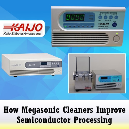
Kaijo can draw on its extensive experience in the megasonic cleaning field to recommend products for specific semiconductor cleaning applications. The company produces high-quality ultrasonic and megasonic equipment ranging from the lowest to the highest frequencies. For example, for superfine wafer cleaning applications, customers should consider Kaijo’s Quava Mega Puck megasonic wafer cleaning system. Kaijo can evaluate customer requirements, make recommendations and ensure that the corresponding equipment delivers the expected benefits to a customer’s semiconductor manufacturing operation.