Optimizing Semiconductor Fabrication with Advanced Megasonic Cleaning
Written by: Site Manager | April 4, 2024
 Because a high level of silicon wafer cleanliness is critical for semiconductor product quality, removing contaminating particles is a crucial feature of semiconductor manufacturing. Microscopic particles clinging to wafer surfaces can block silicon etching or the deposit of conducting paths. The resulting products can be defective or have a reduced lifespan. Reducing the particle count as much as possible results in superior-quality products.
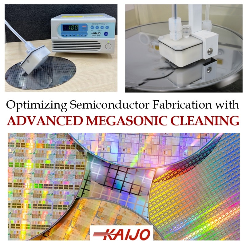
Kaijo’s Quava Mega Puck Flow System removes even the smallest particles from silicon wafer surfaces. Megasonic cleaning at 1.0MHz to 2.0MHz dislodges contaminating particles as water flows through the megasonic transducer puck to wash them away. Semiconductor manufacturing using the Mega Puck wafer cleaning system can achieve higher levels of cleanliness and lower particle counts than alternative cleaning systems.
The Challenges Faced by Process Engineers in Semiconductor Fabrication
A key goal for semiconductor device fabrication is high efficiency with consistent output quality. To achieve this goal, process engineers work with production times, throughput, costs, and product failure rates. Key challenges are to reduce production times and costs while increasing throughput and maintaining the desired product quality.
Effective wafer cleaning is essential for process efficiency because it takes time and affects product defects. When process engineers allocate more time for wafer cleaning, product quality may increase, but process efficiency decreases. At the same time, cleaning needs to provide effective results so the process engineers can be confident that output quality is consistent. A low-cost wafer cleaning system that works quickly and produces low particle counts can help process engineers meet their overall semiconductor fabrication process efficiency goals.
Overview of Megasonic Cleaning Technology
Megasonic cleaning systems use high-frequency sound waves in a cleaning solution to remove contamination from part surfaces. Frequencies in the MHz range create microscopic cavitation bubbles in the cleaning solution. As the bubbles form and collapse in tune with the frequency, they produce a scrubbing action that cleans effectively. The bubbles are especially good at dislodging microscopic particles stuck to wafer surfaces or adhering due to static cling. Megasonic cleaning is fast, cleans thoroughly, and has low operating costs.
Kaijo’s Quava Mega Puck Flow System applies megasonic technology to clean silicon wafers and other large, delicate surfaces. When the puck skims across the silicon wafer, it covers the surface with a cleaning solution and introduces megasonic sound waves underneath the puck. As the wafer rotates, the whole surface is cleaned rapidly by the focused application of sound waves in the cleaning solution. Cavitation bubbles created by the sound waves deliver rapid and effective cleaning, using a cleaning solution to remove contaminating particles.
Features of Kaijo’s Quava Mega Puck Flow System
The Mega Puck Flow system can clean various flat surfaces and components of different sizes. In addition to silicon wafers, the system can clean flat panel display glass, complex disc drive media, and semiconductor equipment components. Key features include:
- 1.0MHz to 2.0MHz operation
- Programmable soft start and soft stop
- 100 to 240 V AC voltage range
- De-ionized water or a chemical solution for cleaning
- Power set-point controls in 0.1Watt increments
- Host PC communication capability
The system is easy to install and does not need field calibration if a megasonic generator or transducer is replaced. It is characterized by a high cleaning solution flow rate, rapid rotation of the substrate to be cleaned, and enough distance between the Puck and the substrate to clear any holding pins.
Tailored Solutions for Semiconductor Manufacturing Challenges
The Mega Puck Flow System offers customization for substrate size and unique cleaning needs. Optional frequency and oscillation modes can be selected to meet specific cleaning requirements. Because the cleaning effort is applied directly to the wafer surface through the cavitation bubbles, minor adjustments and setting variations can significantly affect cleaning performance. Process engineers can tune the system to produce the desired results and optimize it to deliver productivity increases that align with their goals.
Advantages for the Process Engineer
The Mega Puck Flow System provides process engineers with several advantages to increase efficiency and maintain output quality. They can use the wafer cleaning system to reduce cleaning times and cleaning costs while producing clean wafers with a consistently low particle count. Using Kaijo’s Mega Puck Flow System, a semiconductor fabrication process can lower overall processing times. Throughput will increase, and output quality will remain consistent.
Implementing the Quava Mega Puck Flow System
As a compact and flexible silicon wafer cleaning solution, Kaijo’s Mega Puck Flow System can easily be integrated into semiconductor manufacturing lines that need this kind of cleaning. Kaijo offers free pre-ordering consultation to ensure potential customers choose the right system configuration for their application. Once built, Kaijo systems are thoroughly tested before installation. After-sales support is a Kaijo priority. The company can offer qualified service personnel to ensure the system works as expected.
Implementing Kaijo’s Mega Puck Flow System will help process engineers achieve their operational goals, increasing efficiency and product quality. Contact Kaijo to discuss your process requirements or learn how Kaijo’s systems can provide effective solutions.