

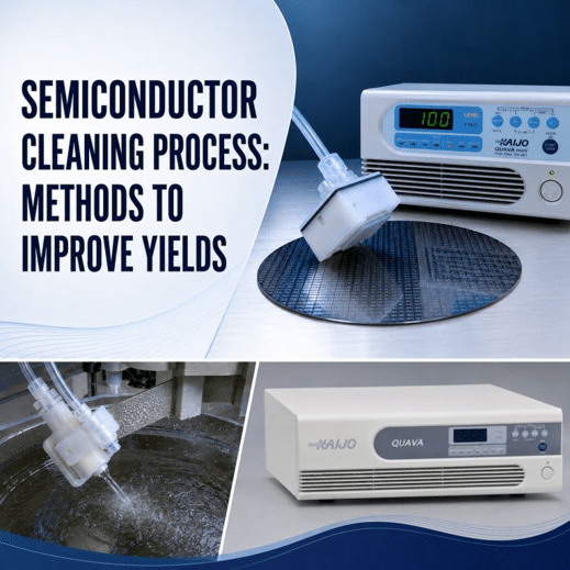
This guide explains what causes contamination on silicon wafers, how wet, dry, ultrasonic, and megasonic cleaning methods compare, and how to choose cleaning equipment that protects yield without slowing your line.
Every fab and R&D facility documents its cleaning protocols in detail, yet particle counts still creep up, chambers still drift out of spec, and engineers still spend hours tracing a yield dip back to a rinse step. The semiconductor cleaning process sits at the center of that tension: it has to remove contamination thoroughly enough to protect increasingly small device geometries, while running fast enough to keep pace with production targets. This page explains where contamination comes from, how the major cleaning methods work, and what to evaluate when your current process or equipment stops keeping up.
Request a Free Process Consultation with Kaijo’s Experts
The Semiconductor Cleaning Process Challenges Engineers Face
A documented semiconductor cleaning process is not the same as a stable one. Even fabs with mature, well-controlled protocols see particle- and residue-related yield loss creep back in. That gap between “documented” and “reliable” is what keeps engineers troubleshooting instead of optimizing. A cleaning step that passed qualification six months ago can drift as tanks age, transducers wear, or chemistry lots vary, and the first sign is often a yield report, not an equipment alarm.
That troubleshooting burden collides with a second pressure: throughput. Cycle-time targets rarely leave room to slow down a cleaning step just because contamination risk has crept up, so engineers are asked to hold cleaning efficacy steady while the line keeps moving. Extending a bath time or adding a rinse cycle protects quality, but it also eats into the very throughput numbers the process is measured against.
Changing equipment or chemistry to fix the problem carries its own risk. Requalifying a cleaning tool or chemistry mid-process means new characterization data, new SPC baselines, and, if something goes wrong, downtime the line can’t easily absorb, so many teams keep running a process they know is imperfect because the alternative is disruption they can’t schedule around.
Underneath both pressures is a subtler problem: inconsistency. The same recipe can produce different results across tools, chambers, or shifts, turning what should be a settled process step into a recurring root-cause investigation. Bath aging, transducer degradation, and chamber-to-chamber variation in agitation energy are common, hard-to-isolate contributors.
The sections below explain where this contamination originates, how major cleaning methods address it, and what to evaluate when it’s time to change equipment rather than keep troubleshooting around it. Kaijo works with process teams as a technology partner on that evaluation, not simply as an equipment vendor, because getting the frequency, power, and cleaner design right for a specific application determines whether a new system actually closes the gap.
Common Sources and Types of Contamination in the Wafer Cleaning Process
Every wafer cleaning process removes four broad categories of contamination, each of which threatens device performance differently.
- Particles — dust, process residue, and abraded material that can bridge circuit features or block subsequent deposition and etch steps.
- Organic residues — photoresist remnants, oils, and other carbon-based films left behind by handling or prior process steps.
- Metallic ions — trace metals (such as iron, copper, or sodium) that diffuse into the silicon lattice and degrade electrical performance or device reliability.
- Native oxides — thin oxide layers that form on exposed silicon after brief exposure to air or moisture, which can interfere with subsequent bonding or contact steps if not removed at the right point in the flow.
These contaminants enter the process from a predictable set of sources: wafer handling (robotic or manual), the purity of process chemicals and rinse water, the cleanroom environment itself (airborne particles, humidity, outgassing), and gradual equipment wear, worn seals, degraded transducers, or aging tanks that shed particles into an otherwise clean bath.
Fabs don’t set their own bar for what counts as “clean”, they’re measured against cleanliness and contamination-control standards published by SEMI, the semiconductor industry’s standards organization, alongside cleanroom air-cleanliness classifications such as ISO 14644. Meeting those benchmarks isn’t optional documentation; it’s the baseline a process must meet before yield conversations even start.
Contamination risk ultimately splits into two related but distinct concerns. For process teams, it’s a direct yield and device-performance issue: particles and metallic ions cause defects that show up in test data. For facilities and operations leadership, the same contamination sources are a regulatory and safety compliance issue. Chemical handling, cleanroom certification, and environmental controls are all audited against the same standards. Solving contamination at the source benefits both.
Core Silicon Wafer Cleaning Methods Explained
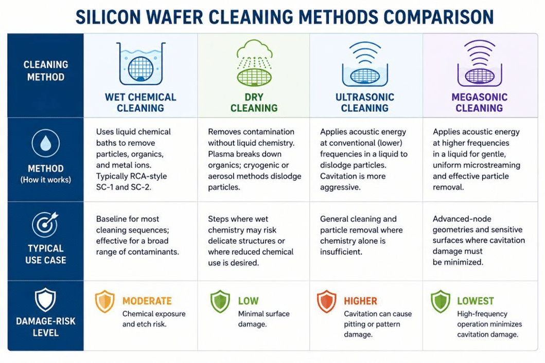
Fabs draw on four main approaches to silicon wafer cleaning, and most production flows combine more than one.
Wet chemical cleaning remains the industry baseline, typically following the RCA-style two-step sequence developed for the industry: a Standard Clean 1 (SC-1) bath — ammonium hydroxide and hydrogen peroxide — targets particles and organic residue, followed by a Standard Clean 2 (SC-2) bath — hydrochloric acid and hydrogen peroxide- targets metallic ion contamination. Wet chemistry is well characterized and effective across a broad range of contaminant types, which is why it anchors most cleaning sequences even as other methods are added around it.
Dry cleaning methods — including plasma, cryogenic, and aerosol cleaning remove contamination without liquid chemistry. Plasma cleaning uses reactive gas plasma to break down organic residues, while cryogenic and aerosol methods use CO2 snow or particle jets to dislodge contaminants. These approaches reduce chemical use and wastewater treatment, making them especially useful where wet chemistry could damage delicate structures.
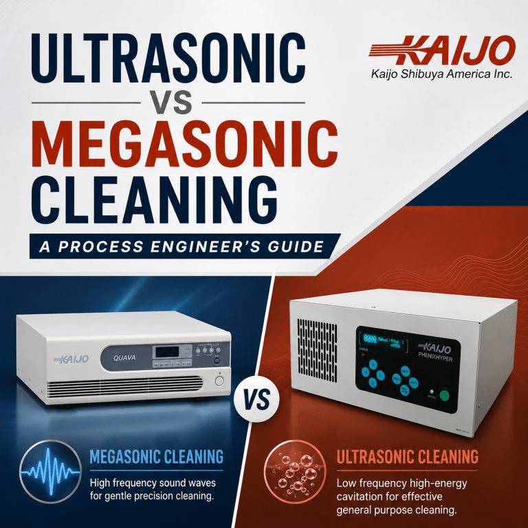
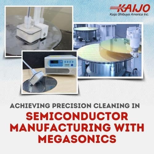
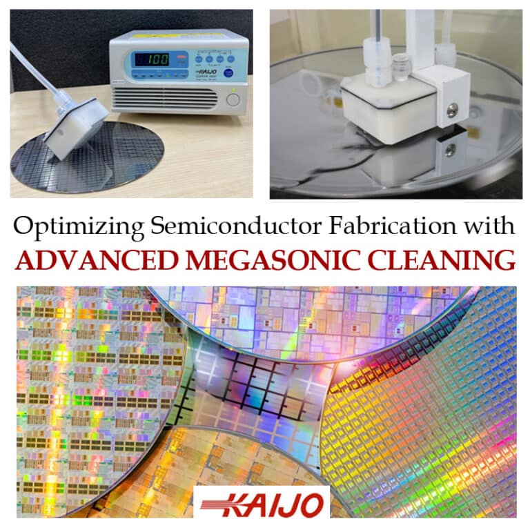
Ultrasonic and megasonic cleaning apply acoustic energy through a liquid medium to dislodge particles that chemistry alone won’t remove. Megasonic cleaning runs at substantially higher frequencies than conventional ultrasonic cleaning, producing gentler, more uniform microstreaming in the liquid instead of the more aggressive cavitation associated with lower-frequency ultrasonic energy. That’s why megasonic cleaning is generally preferred for sensitive wafer surfaces and advanced-node geometries, where cavitation-driven pitting or pattern damage is a real risk, a distinction covered in more depth on Kaijo’s megasonic cleaning systems for semiconductor wafers page.
Which method a fab uses at a given step comes down to tradeoffs: wet chemistry is highly effective but adds chemical handling and disposal steps; dry methods reduce chemical use but can be slower or more limited in contaminant range; ultrasonic and megasonic cleaning add strong particle removal, with a real difference in damage risk between the two depending on frequency. Most cleaning sequences layer these methods rather than choosing just one.
Review the Megasonic System Built for Your Cleaning Method
Batch Cleaning vs. Single-Wafer Cleaning: What’s the Difference?
Once fabs set the cleaning chemistry and method, they still have to decide how wafers move through the process together or one at a time.
Batch cleaning processes multiple wafers together, typically loaded into a cassette and run through shared chemical and rinse tanks. Its main advantage is throughput: cleaning a full cassette of wafers in one bath cycle is far more time and cost-efficient per wafer than processing them individually.
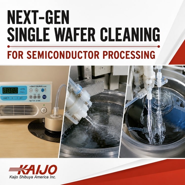
Single-wafer cleaning processes one wafer at a time, usually on a spin chuck with chemistry and rinse delivered by flow or spray. It trades some throughput for precision – each wafer gets consistent, isolated exposure to fresh chemistry, with no risk of cross-contamination from neighboring wafers in a shared bath.
- Factor
Batch cleaning
Single-wafer cleaning - Throughput
Higher — multiple wafers per cycle
Lower — one wafer per cycle - Process control
Shared exposure across the batch
Isolated, wafer-by-wafer control - Cross-contamination risk
Present in shared baths
Minimized by isolation - Typical fit
Legacy nodes, less-critical steps
Advanced-node, critical layers - Cost profile
Lower per-wafer cost
Higher per-wafer cost, higher precision
Where each approach fits often tracks device node and process criticality. Batch cleaning still suits legacy nodes and less-critical steps, where its cost and throughput advantages outweigh the tighter control single-wafer systems provide. As device geometries shrink, single-wafer cleaning increasingly becomes a requirement rather than an option. The tolerances at advanced nodes leave less room for the variability a shared bath introduces.
Because both approaches remain in active use across most fabs, equipment flexibility matters as much as the cleaning chemistry itself. Kaijo’s product range spans both: tank-based ultrasonic systems built for batch processing and megasonic flow systems, including Kaijo’s Mega Puck Flow single-wafer cleaning system, engineered specifically for single-wafer precision cleaning. Rather than forcing a fab to standardize on one architecture, that range lets a process team match the equipment to the step, node, and criticality it’s actually cleaning for.
Review the Specs for the Quava Mega Puck Flow System
A Step-by-Step Look at the Wafer Cleaning Process
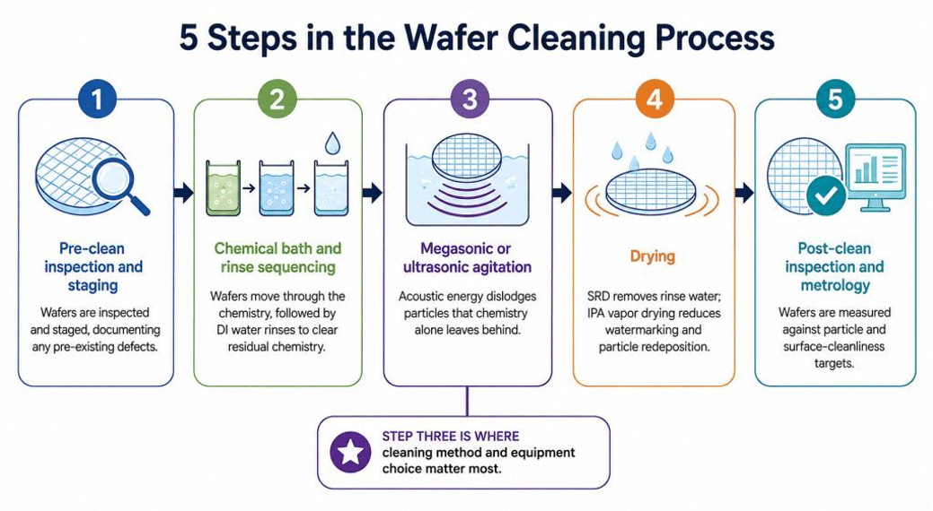
A production wafer cleaning process typically moves through five stages, regardless of the chemistry or agitation method used in a given step.
- Pre-clean inspection and staging. Wafers are inspected and staged before entering the cleaning sequence, so operators document any pre-existing defects rather than mistaking them for a later cleaning failure.
- Chemical bath and rinse sequencing. Wafers move through the chemistry appropriate to the contamination being targeted — wet chemical baths, dry plasma exposure, or a combination — followed by deionized water rinse steps to clear residual chemistry before it can redeposit or react on the surface.
- Megasonic or ultrasonic agitation. Acoustic energy is applied during the bath or rinse step to dislodge particles that chemistry alone leaves behind, with frequency selected to balance particle-removal efficiency against the wafer’s tolerance for cavitation energy.
- Drying. Spin rinse dry (SRD) uses centrifugal force to remove rinse water. In contrast, isopropyl alcohol (IPA) vapor drying displaces water with IPA vapor to reduce watermarking and particle redeposition on more sensitive surfaces.
- Post-clean inspection and metrology. Wafers are measured against particle-count and surface-cleanliness targets before moving to the next process step, confirming the cleaning sequence met its specification rather than assuming it did.
Step three is where cleaning method and equipment choice matter most. Get the agitation energy wrong – too aggressive for the geometry, too weak for the contamination – and steps one and five document the failure instead of preventing it. That’s where systems designed for single-wafer cleaning, as referenced above, maintain a consistent, controlled acoustic profile across every wafer, run after run. That consistency keeps step five from becoming a recurring investigation
Request a Free Process Review with Kaijo’s Experts
Choosing the Right Semiconductor Cleaning Equipment and Technology
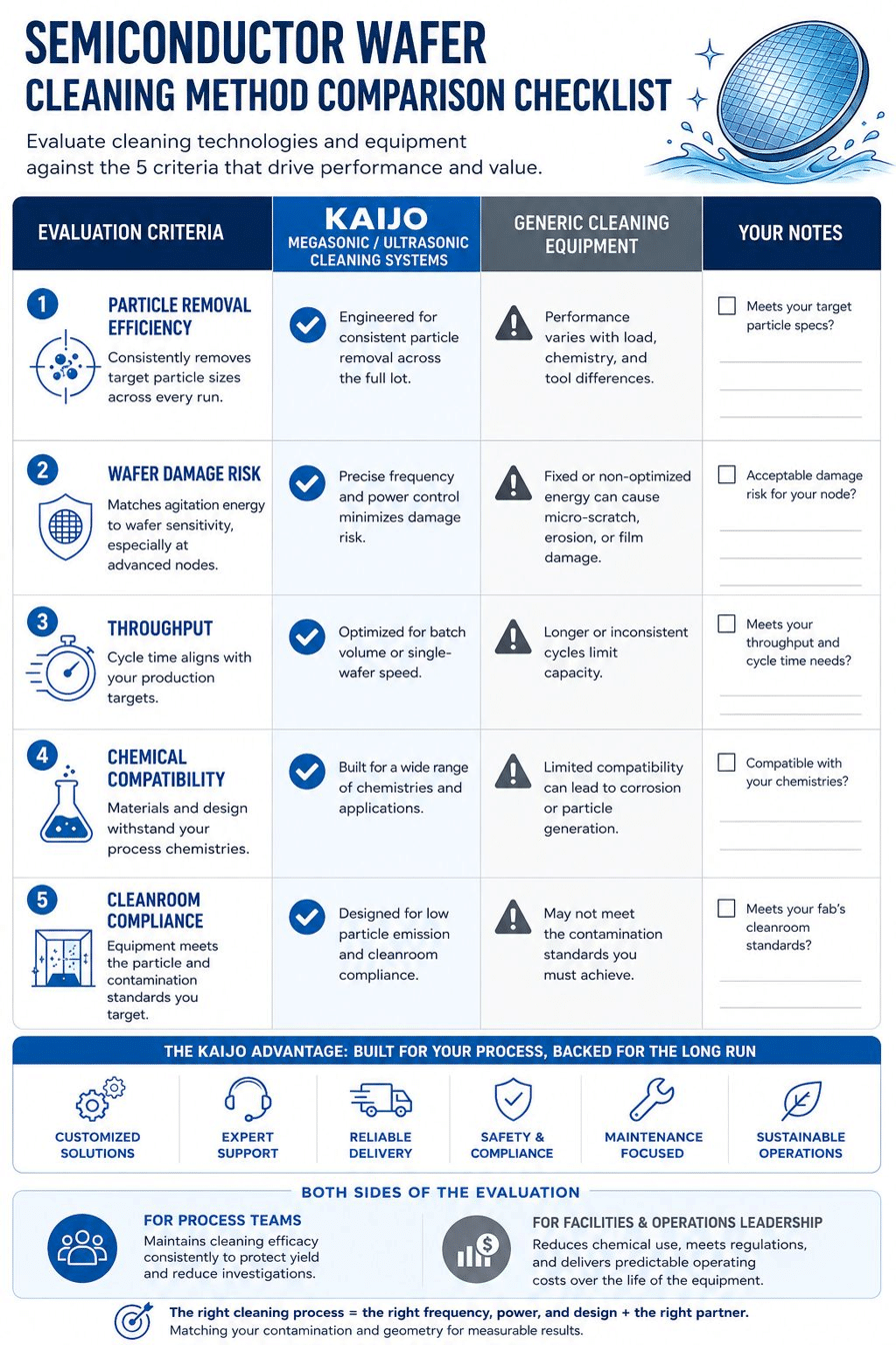
Selecting equipment for a semiconductor cleaning process comes down to five evaluation criteria that matter regardless of fab size or device node:
- Particle removal efficiency — how consistently the system clears target contaminant sizes across a full run, not just in qualification testing.
- Wafer damage risk — whether the agitation energy is matched to the wafer’s structural sensitivity, particularly at advanced nodes.
- Throughput — how the system’s cycle time fits your production targets, whether that means batch volume or single-wafer speed.
- Chemical compatibility — whether the system’s materials and design hold up to the specific chemistries in your process flow.
- Cleanroom compliance — whether the equipment itself meets the particle and contamination standards it’s supposed to help you hit.
Kaijo’s megasonic and ultrasonic cleaning systems are engineered around these five criteria directly, rather than adapted from general-purpose industrial cleaning equipment. Frequency, power level, and cleaner design match the application, batch or single-wafer, particle-sensitive or metal-sensitive instead of applying one configuration across every use case.
What separates Kaijo from generic cleaning equipment is less about any single spec and more about the surrounding support: systems customized to specific fab requirements, technical support through qualification and beyond, delivery assurance, safety compliance built into the equipment design, and maintenance practices aimed at holding performance steady over years of use rather than degrading between service visits.
That combination addresses both sides of the evaluation. For process teams, it’s an efficiency and quality question. Does the system maintain cleaning efficacy consistently enough to stop yield investigations before they start? For facilities and operations leadership, it’s a cost, compliance, and sustainability question. Does the equipment reduce chemical consumption, meet regulatory requirements, and keep operating costs predictable over its service life?
Getting the semiconductor cleaning process right is rarely about one dramatic equipment change. It’s about matching frequency, power, and design to the specific contamination and geometry you’re working with, and having a partner who’ll work through that matching with you rather than sell you a standard configuration.
Request a Free Consultation with Kaijo’s Experts
Articles & Resources:
Learn More about Improving Semiconductor Cleaning Processes:
Frequently Asked Questions
The most reliable improvements come from matching the cleaning method — wet chemical, dry, ultrasonic, or megasonic — to the specific contamination type and wafer sensitivity at each step, rather than applying one method across the whole flow. Tightening bath control, monitoring transducer performance, and validating cleanliness with post-clean metrology also reduce the drift that causes step-by-step results to vary. See the equipment evaluation criteria above for what to check when equipment is the limiting factor.
Wet chemical cleaning uses liquid chemistry — such as RCA-style SC-1/SC-2 baths — to remove particles, organic residue, and metallic ions, and remains the most broadly effective method. Dry cleaning methods, including plasma and cryogenic/aerosol cleaning, remove contamination without liquid chemistry, reducing chemical consumption and wastewater but offering a narrower range of contaminants on their own.
Particles can bridge circuit features or interfere with deposition and etch steps; metallic ions can diffuse into the silicon lattice and degrade electrical performance and reliability; organic residues and native oxides can interfere with bonding and contact steps if not removed at the right point in the process. Each contaminant type creates a different failure mode, which is why contamination is tracked by category rather than as a single generic metric.
There is no single interval; it depends on your equipment, process chemistry, and internal SPC requirements. Kaijo's team can help define a schedule for your system during onboarding and ongoing support.
Next Steps for Your Cleaning Process
A stable semiconductor cleaning process comes from matching contamination type, wafer sensitivity, and equipment design, not from picking a single method and hoping it covers every step. If particle counts, cross-tool variability, or qualification risk are driving your team back into troubleshooting mode, it may be time to evaluate whether your current cleaning equipment still matches what you’re cleaning.
Process & Yield
If bath aging, transducer wear, or chamber-to-chamber variability is turning a settled process step into a recurring root-cause investigation, the fix usually isn’t a bigger fix to the same equipment—it’s matching frequency, power, and cleaner design to what you’re actually cleaning. Kaijo’s megasonic and ultrasonic systems are built around the five evaluation criteria above, so the question is whether your current equipment still holds up.
See How Kaijo’s Systems Improve Wafer Yield
Facility Compliance & Cost
Contamination control isn’t only a yield question, it’s also what your fab gets audited against. Chemical handling, cleanroom certification, and environmental controls all fall under the same SEMI and ISO 14644 standards discussed above, and the equipment you run affects chemical consumption, regulatory risk, and operating cost over its service life. If your team is weighing a cleaning system change against compliance requirements or cost targets rather than yield alone, Kaijo’s team can walk through what that evaluation should look like for your facility.