


Next-Gen Wafer Cleaning Systems for Single-Wafer Semiconductor Processing
Written by: Michael Danese | August 11, 2026
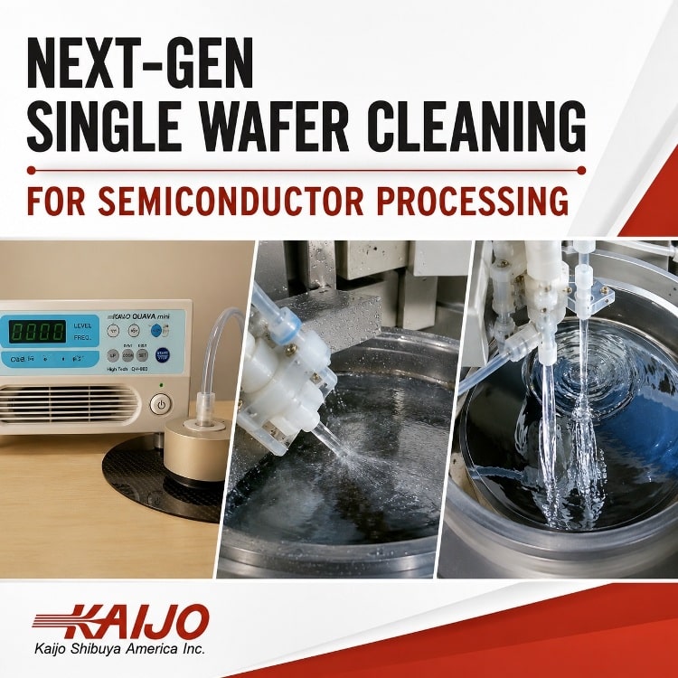 As device geometries shrink below 3nm, single-wafer cleaning has become critical to yield and device reliability in modern wafer cleaning systems. This article explains the process challenges faced by R&D and fabs and how Kaijo’s megasonic QUAVA systems and engineering support address them.
Table of Contents
- The Growing Complexity of Single Wafer Cleaning in Semiconductor Manufacturing
- Critical Wafer Cleaning Process Challenges That Impact Yield and Throughput
- How Megasonic Wafer Cleaning Systems Address Single Wafer Process Challenges
- Kaijo’s Advanced Single Wafer Cleaning Systems for Every Process Need
- Process Consulting and Custom Solutions to Optimize Your Wafer Cleaning Strategy
- Frequently Asked Questions
1. The Growing Complexity of Single Wafer Cleaning in Semiconductor Manufacturing
Semiconductor fabs and R&D facilities have largely moved away from batch cleaning in favor of single wafer processing. The reason comes down to process control, not fashion.
Batch tanks clean many wafers simultaneously using shared chemistry. That chemistry doesn’t stay constant: it depletes and picks up dissolved contaminants as more wafers pass through, so a wafer cleaned early in a run doesn’t see quite the same conditions as one cleaned near the end. Wafers sharing a bath can also contaminate each other.
Single wafer systems avoid this by draining and refreshing chemistry between wafers and applying a distinct recipe to each one, an approach memsstar’s comparison of single wafer and batch processing points to directly: wafers processed together in a shared chamber begin to influence one another, which is why single wafer methods win out whenever higher uniformity and yield are required. That per-wafer flexibility also matters in fabs running several product types through the same line. And because single-wafer modules typically sit inside vacuum-compatible cluster tools alongside etch and deposition steps, wafers spend less time exposed to ambient air between process steps, thereby closing another contamination pathway.
For a closer look at how these two approaches compare across contamination control, throughput, and equipment cost, see the section titled “Batch Cleaning vs. Single-Wafer Cleaning: What’s the Difference?” on the “Semiconductor Cleaning Process: Methods to Improve Yields” application page.
As device geometries shrink to 3nm, 2nm, and beyond, a single stray particle or trace metallic ion can be enough to kill a die.
Cleanliness requirements that once tolerated micron-scale particles now demand control at the sub-nanometer level. At these tolerances, a wafer cleaning system is directly tied to yield, device reliability, and the repeatability that high-volume manufacturing depends on.
Contamination comes from several sources: particulates left behind from etch and deposition steps, metallic ions that diffuse into the silicon and compromise device performance, organic residues from photoresist and cleaning chemistries, and native oxides that form on exposed surfaces between process steps.
Traditional cleaning methods, designed for larger geometries and more forgiving defect budgets, struggle to keep pace. Brush scrubbing risks mechanical damage to delicate features. Wet chemical baths alone often can’t reach sub-micron particles lodged in high-aspect-ratio structures.
2. Critical Wafer Cleaning Process Challenges That Impact Yield and Throughput
For process engineers and R&D teams, the challenges of single-wafer cleaning show up daily, often as the difference between a good lot and a scrapped lot. Particle contamination at the sub-micron and nano-scale remains one of the most significant yield killers in modern wafer fabs. A wafer cleaning system that can’t consistently remove particles at this scale puts every downstream process step at risk.
Chemical compatibility adds another layer of difficulty. Engineers need chemistries aggressive enough to dissolve contaminants but gentle enough to leave sensitive device structures, including thin films, high-aspect-ratio features, and delicate interconnects, untouched. Get the balance wrong, and cleaning itself becomes a source of defects: micro-scratching, pattern damage, and stress-induced failures from overly aggressive mechanical or chemical methods.
Consistency compounds the problem. High-volume manufacturing demands that cleaning results repeat reliably across every wafer in every batch, and as defect density requirements tighten with each new node, there’s less room for variation. On top of the technical challenges sit operational pressures: fabs need to balance cleaning effectiveness against throughput targets, water consumption, and chemical costs, all while integrating new technology without disrupting existing workflows.
These pressures are why megasonic cleaning has become the preferred approach for precision single-wafer applications.
3. How Megasonic Wafer Cleaning Systems Address Single Wafer Process Challenges
Megasonic cleaning uses high-frequency acoustic waves, generally classified by Kaijo and other manufacturers as ranging from 950 kHz to 3 MHz, transmitted through a liquid medium to dislodge surface contaminants without mechanical contact. It’s a fundamentally different mechanism than traditional ultrasonic cleaning, which operates at lower frequencies. The higher frequencies used in megasonic cleaning produce shorter wavelengths and more controlled cavitation, which translates directly into a lower risk of wafer damage.
The physics behind particle removal comes down to acoustic streaming and micro-agitation. The acoustic energy lifts contaminants off the wafer surface rather than blasting them off, avoiding the abrasion risk associated with harsher methods. This makes megasonic cleaning compatible with DI water and a wide range of process chemistries, so it integrates into existing wet-process flows without requiring a redesign.
Compared with wet-chemical-only and other cleaning processes, megasonic cleaning offers better particle removal efficiency, reduced chemical consumption, lower water usage, and more repeatable results. All of these matter to fabs and R&D facilities that balance cleanliness against operational costs.
Frequency selection matters as much as the technology itself. Lower frequencies in the mid-sonic range, such as 430 kHz, are better suited to heavier contamination, where more aggressive energy is needed to dislodge larger particles. Higher frequencies, from 950 kHz up to 3 MHz, are the better fit for delicate structures and fine-feature cleaning, where minimizing energy is the priority.
Explore Kaijo’s full line of megasonic cleaning systems to see how frequency and power are matched to specific process needs.
4. Kaijo’s Advanced Single Wafer Cleaning Systems for Every Process Need
Kaijo Shibuya has more than 70 years of experience in engineering ultrasonic and megasonic cleaning technology, and that depth of experience shows in the QUAVA family of megasonic wafer cleaning transducers. Each QUAVA system is built to solve a specific process problem rather than serve as a one-size-fits-all tool.
| System | Frequency / Power | Housing / Transducer | Best For |
| QUAVA Spot Shower | 430 kHz, 950 kHz, 2 MHz, or 3 MHz; adjustable 1–50W output | Field-configurable for DI water use | Precise, damage-free single wafer cleaning with DI water |
| QUAVA Indirect Spot Shower | 430 kHz or 950 kHz | PTFE housing (SUS, PCTFE also available) | Foaming chemistries and high-temperature processes; isolates energy source from chemical flow |
| QUAVA Mega Puck | 950 kHz; adjustable up to 100W | Quartz, sapphire, or stainless-steel transducer plate; SUS/ECTFE body | Stable, uniform acoustic energy across diverse process needs |
| QUAVA Mega Wedge | 950 kHz or 3 MHz, high-power options | PEEK housing (SUS also available) | Aggressive contamination removal on advanced nodes |
The QUAVA Indirect Spot Shower transmits megasonic energy through a quartz plate, keeping the energy source separate from the chemical flow. This minimizes bubble formation and heat generation while supporting the simultaneous delivery of DI water and chemical solutions. The QUAVA Mega Wedge enables contactless wafer cleaning via a quartz or sapphire transducer plate, with DI water or a chemical solution applied separately, providing maximum flexibility in chemistry selection.
Across the QUAVA line, Kaijo provides process engineers with a wafer-cleaning system configuration matched to the contamination type, chemistry, and device sensitivity of their specific application. See full specifications for the QUAVA Spot Shower and QUAVA Mega Puck.
5. Process Consulting and Custom Solutions to Optimize Your Wafer Cleaning Strategy
Choosing the right cleaning technology is only part of the equation. Configuring it correctly for a specific process is where results are won or lost. Kaijo’s engineering team works directly with process engineers, R&D teams, and OEM integrators to identify the right wafer cleaning system configuration for each application, rather than handing off a generic product and walking away.
That partnership starts with process analysis: Kaijo evaluates existing cleaning workflows to identify inefficiencies, contamination sources, and opportunities for optimization before recommending a solution. For applications that don’t fit an off-the-shelf configuration, Kaijo’s custom wafer-cleaning solutions let engineers specify unique frequency, power, housing material, and nozzle configurations tailored to their exact process requirements.
The payoff extends beyond cleaning performance. Kaijo’s megasonic cleaning systems help fabs reduce water, chemical, and energy costs, supporting both operational budgets and sustainability goals. And because Kaijo maintains active partnerships throughout the product lifecycle, engineers get ongoing technical support rather than a one-time transaction.
If your current process is struggling to meet yield or repeatability targets, or you’re designing a new single wafer cleaning process from the ground up, Kaijo’s engineering team can help.
Explore the benefits and capabilities of Kaijo’s full line of QUAVA megasonic wafer cleaning systems. Schedule a free process consultation with Kaijo’s technical team to evaluate your current wafer cleaning process and identify the right QUAVA system for your application.
6. Frequently Asked Questions
1. What is megasonic cleaning and how does it differ from standard ultrasonic cleaning for semiconductor wafers?
Megasonic cleaning uses frequencies generally in the 950 kHz to 3 MHz range, while ultrasonic cleaning ranges from 26 kHz up to 200 kHz. The higher frequencies produce shorter wavelengths, more controlled acoustic streaming, and far less cavitation energy, resulting in effective particle removal with minimal risk of wafer damage. This makes megasonic cleaning the preferred method for precision semiconductor wafer applications.
2. Which QUAVA wafer cleaning system is best suited for processes involving foaming or high-temperature chemistries?
The QUAVA Indirect Spot Shower is specifically engineered for foaming and high-temperature chemical applications. Its quartz plate design isolates the transducer from the chemical flow, minimizing bubble formation and thermal interference while still delivering effective megasonic energy to the wafer surface.
3. How does megasonic cleaning prevent damage to sensitive wafer features and advanced device structures?
Megasonic cleaning removes particles through acoustic streaming, a gentler, non-contact mechanism, rather than aggressive cavitation. By selecting the appropriate frequency and output power for the specific process, engineers can tune the energy level to maximize particle removal efficiency while staying well below the threshold that could damage fragile device features or thin films.
4. What frequency and power options are available in Kaijo’s QUAVA wafer cleaning system product line?
Kaijo’s QUAVA line spans 430 kHz to 3 MHz depending on the model, with power outputs adjustable up to 100W in 0.1W increments. Transducer plate materials include quartz, sapphire, and stainless steel, with housing options in PEEK, PTFE, PCTFE, ECTFE, and SUS. Exact options vary by model. See the comparison table above or contact Kaijo for a configuration matched to your process.
5. How can Kaijo’s process consulting services help optimize our current wafer cleaning process?
Kaijo’s engineering team offers process analysis consultations to evaluate existing cleaning workflows, identify contamination sources, and recommend the optimal configuration for the wafer cleaning system. Whether you’re designing a new process from scratch or troubleshooting yield losses in an existing fab, Kaijo works directly with your team or your OEM integrator to develop a tailored solution. Contact Kaijo to schedule a free consultation.