



Ultrasonic vs. Megasonic Cleaning: A Process Engineer’s Guide
Written by: Michael Danese | July 7, 2026
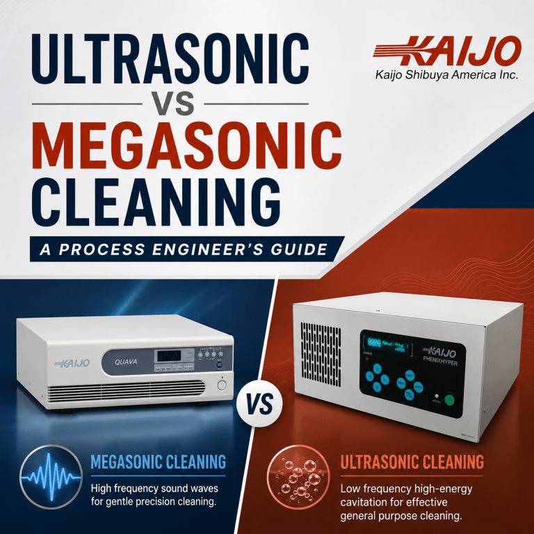 This article compares industrial ultrasonic and megasonic cleaning systems across frequency, cavitation behavior, energy density, particle removal efficiency, substrate sensitivity, chemical compatibility, and process integration — giving process engineers the technical criteria to specify the right system for their semiconductor or industrial cleaning application.
Table of Contents
- What Ultrasonic and Megasonic Cleaning Have in Common
- Key Differences: Frequency Range, Cavitation Behavior, and Energy Density
- Substrate Sensitivity: When Megasonic Cleaning Is Required vs. When Ultrasonic Is Sufficient
- Particle Removal Performance at Different Feature Sizes
- Chemical Compatibility Considerations for Each Technology
- Process Integration: Batch vs. Single-Wafer Cleaning Systems
- Matching the Right Ultrasonic or Megasonic System to Your Cleaning Application
- FAQ: Ultrasonic vs. Megasonic Cleaning
Introduction
Specifying the wrong acoustic cleaning technology at an advanced process node doesn’t produce a marginal yield loss; it produces a systematic one. The decision between industrial ultrasonic cleaners and megasonic cleaning systems is determined by substrate geometry, target particle size, and process integration requirements — not cleaning intensity alone. This guide compares the two technologies across frequency, cavitation behavior, energy density, substrate sensitivity, particle removal efficiency, chemical compatibility, and process integration, drawing on Kaijo Shibuya’s engineering experience in both technology categories.
1. What Ultrasonic and Megasonic Cleaning Have in Common
Both ultrasonic cleaners and megasonic cleaning systems use piezoelectric transducers driven by electronic generators to introduce acoustic energy into a liquid cleaning medium. Key shared characteristics:
- Non-contact cleaning — eliminates mechanical abrasion risks associated with brush or spray approaches
- Acoustic energy delivery — mechanical agitation generated by acoustic waves reaches internal surfaces, recessed features, and geometries inaccessible to spray or immersion cleaning alone
- Chemistry flexibility — compatible with DI water, aqueous chemistry, or solvent-based solutions
- Process control — power, frequency, and bath chemistry must be carefully managed to avoid substrate damage
The technology decision rests on substrate type, feature geometry, target particle size, and process integration requirements. For a technical overview, see Kaijo’s resource on ultrasonic cleaning technology.
2. Key Differences: Frequency Range, Cavitation Behavior, and Energy Density
Every performance difference between the two technologies — cavitation intensity, energy density, particle removal capability, substrate compatibility — traces back to operating frequency.
Industrial ultrasonic systems typically operate between 20 kHz and 200 kHz. Megasonic systems operate at 950 kHz to 3 MHz, a range that produces fundamentally different acoustic behavior in the cleaning bath.
Cavitation behavior:
- Ultrasonic cleaning systems produce aggressive cavitation — large, energetic bubble collapse events generating intense localized pressure and temperature, highly effective at dislodging bulk contamination from robust surfaces
- Megasonic cleaning systems produce micro-streaming and smaller acoustic bubbles — gentler on substrates while still providing effective particle dislodgment through fluid movement and boundary layer disruption
Ultrasonic systems deliver higher energy density per unit area and are effective for robust industrial parts, but problematic for nanoscale semiconductor structures. The comparison table below summarizes key operating parameters side by side.
| Parameter | Industrial Ultrasonic Cleaning | Megasonic Cleaning |
| Frequency Range | 20 kHz – 200 kHz | 950 kHz – 3 MHz |
| Primary Mechanism | Aggressive cavitation | Acoustic streaming / micro-streaming |
| Cavitation Intensity | High | Low to moderate |
| Energy Density | Higher per unit area | Lower, more controlled |
| Particle Removal Target | 1–10 micron range | Sub-100 nm range |
| Substrate Suitability | Robust industrial parts, mature node wafers | Advanced node wafers, fragile thin films |
| Typical Applications | Machine parts, medical tools, HDD media, LCD glass | Semiconductor wafers, post-CMP, patterned substrates |
Kaijo’s systems, including the Quava series and Phenix line, are engineered to deliver precise, tunable acoustic energy across both frequency ranges, giving process engineers the control needed to optimize performance for their specific application.
3. Substrate Sensitivity: When Megasonic Cleaning Is Required vs. When Ultrasonic Is Sufficient
The core question in cleaning system selection is not which technology cleans more effectively in absolute terms — it’s which technology cleans effectively without damaging the substrate.
When industrial ultrasonic cleaning is sufficient:
- Blank silicon wafers
- Carrier boats, process fixtures, quartz components, and equipment parts where surface topology is not at risk
- Applications where particles in the micron range are the primary contamination target
- Hard disk media, LCD glass, and photovoltaic substrates where moderate acoustic energy is appropriate
When megasonic cleaning is required:
- Silicon wafers where gate structures and high-aspect-ratio features are highly sensitive to cavitation-induced stress
- Substrates with thin-film coatings, fragile metal interconnects, or patterned photoresist that cannot withstand aggressive acoustic energy
- Post-CMP cleaning steps where both particle removal and surface integrity are simultaneously critical
- Applications requiring sub-micron particle removal without introducing new surface defects
The selection calculus is not cleaning effectiveness in isolation — it’s matching acoustic energy output to substrate tolerance at each process step. Kaijo’s engineering team can help process engineers determine which technology, or combination, is appropriate at each step of their cleaning workflow.
| Need Help Matching the Right Cleaning Technology to Your Process?
Kaijo’s experts work directly with process engineers to configure ultrasonic and megasonic cleaning systems for specific substrates, particle sizes, and integration requirements. Get the right answer before you spec your next system. |
4. Particle Removal Performance at Different Feature Sizes
Acoustic frequency directly determines the effective particle removal size. Lower-frequency ultrasonic systems target particles in the 1–10-micron range via cavitation; higher-frequency megasonic systems address sub-100-nm particles via acoustic streaming and microstreaming.
As process nodes shrink, the critical particle size threshold decreases proportionally; particles harmless at 28nm become yield-killing defects at 5nm.
Process engineers should evaluate these three metrics together:
- Particle Removal Efficiency (PRE) — percentage of target particles removed per cleaning cycle
- Defect density — measured before and after cleaning to confirm net contamination reduction
- Wafer surface roughness — assessed post-cleaning to confirm the absence of acoustic damage
A process that achieves high PRE while increasing surface roughness or defect density delivers a net negative yield outcome. Aggressive ultrasonic cleaning can introduce surface damage that offsets the PRE gain, disqualifying it from advanced-node cleaning steps.
Kaijo’s megasonic systems, including the Quava Mega Puck Flow silicon wafer cleaning system, are engineered to achieve high PRE on sub-micron particles while preserving the surface integrity of advanced node substrates.
5. Chemical Compatibility Considerations for Each Technology
Both technologies support a range of cleaning chemistries, but the interaction between acoustic energy and chemistry differs in ways that affect substrate compatibility and process cost.
Ultrasonic chemistry considerations:
- Compatible with aqueous alkaline cleaners, solvent-based solutions, and acidic chemistries for oxide removal
- Cavitation intensity accelerates chemical activity — beneficial for gross contamination but requires careful management to avoid over-etching sensitive substrates
- Detergent concentration and bath temperature must be controlled for repeatable results
Megasonic chemistry considerations:
- Commonly used with DI water, dilute SC-1 (APM), SC-2 (HPM), and dilute HF
- Acoustic streaming enhances chemical transport to the substrate surface at lower concentrations — reducing chemical consumption and waste
- Gentler acoustic energy reduces chemistry-assisted surface damage risk, broadening compatibility with advanced substrate types
For process engineers managing chemical consumption and waste disposal costs, the ability to maintain cleaning effectiveness at lower reagent concentrations directly improves operational efficiency, reducing both chemistry spend and effluent treatment requirements.
Kaijo’s engineering team can assist in optimizing chemistry-equipment combinations for specific semiconductor cleaning requirements.
6. Process Integration: Batch vs. Single-Wafer Cleaning Systems
Batch cleaning systems:
- Process multiple wafers simultaneously in a tank or cassette configuration
- Used in batch configurations for upstream cleaning steps, carrier cleaning, and mature node wafer processing
- Higher throughput per cycle; suited for applications where per-wafer uniformity requirements are less stringent
- Kaijo offers batch-compatible ultrasonic systems through the Phenix line and configurable tank solutions
Single-wafer cleaning systems:
- Process one wafer at a time using megasonic transducers in spin configurations or precision nozzle and puck designs
- Required where wafer-to-wafer uniformity, defect control, and process traceability are critical
- Enables tighter process control and integration into automated fab workflows
- Kaijo’s Quava Mega Puck and Quava Spot Shower systems are purpose-built for single-wafer megasonic cleaning in semiconductor fabs
The configuration decision follows the process requirement: batch systems, where per-wafer uniformity tolerances allow shared-bath processing; single-wafer systems, where wafer-level traceability, uniformity specifications, and advanced-node defect targets cannot be met in a shared-bath environment.
Footprint, automation compatibility, chemical delivery, and process monitoring all factor into system selection. Engaging with Kaijo’s experts ensures configuration aligns with fab workflow and process specifications.
7. Matching the Right Ultrasonic or Megasonic System to Your Cleaning Application
Kaijo Shibuya brings over 75 years of ultrasonic and megasonic engineering expertise to semiconductor and industrial cleaning applications, offering both technology categories from a single engineering partner.
Megasonic systems for semiconductor applications:
- Quava Mega Puck Flow — single-wafer megasonic cleaning with precision flow control for advanced node environments
- Quava Mega Puck — uniform megasonic energy across the wafer surface for consistent particle removal
- Quava Spot Shower — targeted megasonic delivery for precision spot cleaning
- Quava Megasonic Cleaning System — 1200W generator operating from 200 kHz to 950 kHz, effective for sub-micron particle removal from delicate components
- Quava Mini Megasonic Cleaning System — tabletop turn-key system from 200 kHz to 1.6 MHz for precise single- and multi-frequency cleaning applications
- US Shower and Mega Tube — versatile megasonic solution for semiconductor and flat panel display applications
Ultrasonic systems for industrial applications:
- Phenix III Turn-Key Ultrasonic Cleaning System — ready-to-use platform for automotive, aerospace, medical, and electronics manufacturing
- Phenix+ Industrial Ultrasonic Generator — touch-panel controlled with automatic environmental adjustment and uniform wave distribution
- Phenix Legend II — engineered for precision cleaning of hard disk media, flat panel glass, and medical devices
Kaijo differentiators:
- Dual-technology expertise — ultrasonic and megasonic systems from one engineering partner
- Application engineering support from specification through integration
- Water Resonance System (WRS) — a proprietary Kaijo innovation that increases the cavitation effect by over 500%, unavailable from generic equipment suppliers
- Proven applications across semiconductor, HDD, LCD, photovoltaic, medical, automotive, and aerospace
To discuss your specific cleaning application, contact Kaijo to schedule a time to talk with our team of experts.
Contact Usfor a Free Consultation
8. FAQ: Ultrasonic vs. Megasonic Cleaning
Q1. What is the main difference between ultrasonic and megasonic cleaning for semiconductor wafers?
Ultrasonic systems operate at 20 kHz–200 kHz and use aggressive cavitation to dislodge contamination; megasonic systems operate at 950 kHz-3 MHz and produce acoustic streaming, which is gentler on substrates yet still effective at particle removal. For advanced node wafers, cavitation at lower frequencies can damage fragile gate structures and thin-film features that megasonic energy leaves intact.
Q2. At which process node does megasonic cleaning become necessary rather than ultrasonic cleaning?
Sub-28nm is the general threshold at which cavitation damage risk increases significantly for patterned substrates. At 10nm and below, sub-100nm particle removal requirements cannot be reliably met by ultrasonic systems without introducing surface damage.
Q3. Can ultrasonic cleaning damage semiconductor wafers or circuit patterns?
Yes — cavitation at lower frequencies can damage high-aspect-ratio structures, thin-film interconnects, and patterned photoresist on advanced node wafers. Ultrasonic cleaning remains appropriate for carrier cleaning, process fixtures, and mature-node wafer processing where the substrate topology is not at risk.
Q4. What chemistries are compatible with megasonic cleaning systems for wafer processing?
Megasonic systems are commonly paired with DI water, dilute SC-1 (APM), SC-2 (HPM), and dilute HF. Acoustic streaming improves chemical transport to the substrate surface, enabling effective cleaning at lower concentrations and reducing both chemical cost and waste.
Q5. Does Kaijo offer both ultrasonic and megasonic systems for semiconductor manufacturing?
Yes. Kaijo’s megasonic portfolio includes the Quava Mega Puck, Quava Mega Puck Flow, Quava Spot Shower, Quava Megasonic Cleaning System, and Quava Mini Megasonic Cleaning System for semiconductor cleaning; ultrasonic platforms include the Phenix III, Phenix+, and Phenix Legend II for batch and industrial applications. Working with one engineering partner across both technology categories simplifies specification, integration, and ongoing process support.